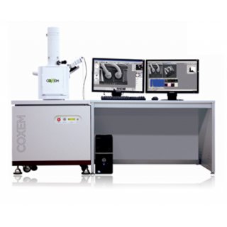
CX-200 TA
The scanning electron microscope (SEM) is the most commonly used tool in surface metrology and is widely used in educational, R&D and quality control programs. Since its invention, electron microscope has been a valuable tool in the
development of scientific theory and has contributed greatly to biology, medicine and material science. This wide spread use of electron microscopes is based on the fact that they enable the observation and characterization of materials on a nanometer (nm) to micrometer (µm) scale. SEM images can yield information about the topography (surface features of an object), morphology (shape and size of the particles making up the object), composition (the elements and compounds that the object is composed of and the relative amounts of them) and crystallographic information (how the atoms are arranged in the object. There are many commercial SEMs in the market with various capabilities and resolutions, however the SEM from CoXem is a powerful tool for surface characterization which allows to capture high resolution images with nano-scale resolution on a varietly of materials.
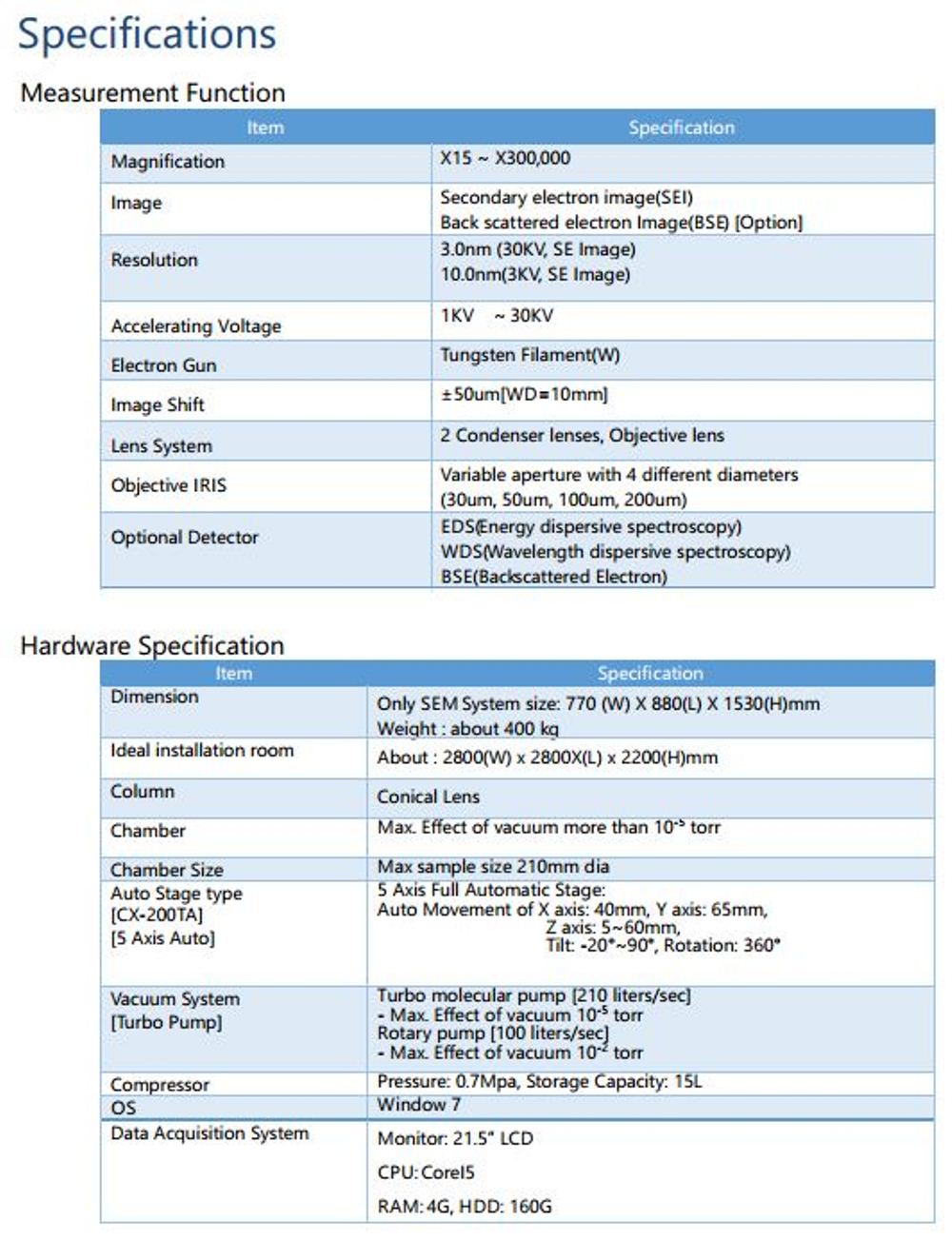
Magnification Range: ~ 15 x – 300,000x
Fully Motorized – All Axis
Stage: X axis: 40mm, Y axis: 65mm, Z axis: 0~60mm, Tilt: -20°~90°
Stage Rotation: 360°
Accelerating Voltage: 1KV ~ 30KV
Image: Secondary Electron Image (SEI)
Resolution: 3.0nm (30KV, SE Image) 10.0nm(3KV, SE Image)
Sample size: 60 mm (D), 45 mm (H)
Optional Detectors:
EDS(Energy dispersive spectroscopy)
WDS (Wavelength dispersive spectroscopy)
BSE(Backscattered Electron)