About ACST
Legal Activity
copyright 2016 - Wit Source Technology Witty
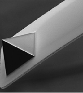
These probes are designed for conducting scanning probe microscopy (C-AFM), Oxidation lithography, E-Chem AFM, Piezo-Force microscopy and SSRM. These probes feature high electrical conductivity and they are not like the metal coated probes. These probes are totally conductive. Additionally, the apex of less than 10 nm radius is respectively sharp when compared to the metal coated probes which gives unprecedented topographic and electrical resolution. Here are the properties of these tips:
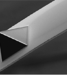
These probes are designed for non-contact imaging, C-AFM, oxidation lithography, nano-indentation and nano-scratching applications. Can be used also for imaging in contact mode in air or liquid on hard surfaces. Here are the properties of these tips:
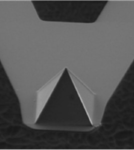
These probes are designed for contact imaging on soft material. Thanks to their ultra-small diamond structure, their surfaces are extremely smooth and exhibit low friction, yet they retain the extreme wear and chemical resistance and inertness, which is critical when imaging soft material. Here are the properties of these tips:
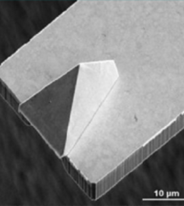
These probes are designed for Scanning Spreading Resistance Microscopy (SSRM) which enables simultaneous topographic imaging and 2D carrier density mapping on the surface of semiconductor samples. In addition these probes can be used for nano-indentation and nano-scratching applications. These probes can be used for imaging in contact mode, in air, liquid, on hard surfaces and non-contact mode. Here are the properties of these tips:
copyright 2016 - Wit Source Technology Witty