COSMOS nanoFAB
Finally, one nano fabrication tool that can do so much more!!
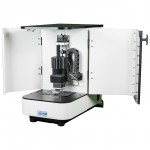
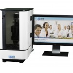
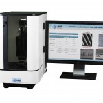
ACST brings to researchers and educators one of its kind, an advanced and multi-purpose desktop micro and nanofabrication instrument that can serve as a research and education too. While it will allow researchers to take their existing work in different directions, it will enable educators to lay a strong foundation for students to master industrially useful micron and nano fabrication techniques. COSMOS nanoFAB is a fabrication platform, and is essential to our nano-SCIENTIST™ educational program that prepares students for the abundant opportunities in the growing field of microfabrication and Nanotechnology.
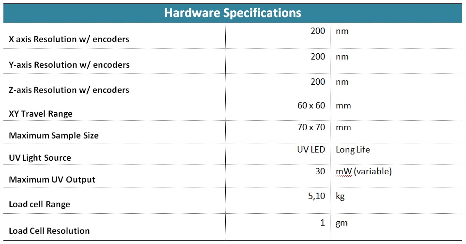
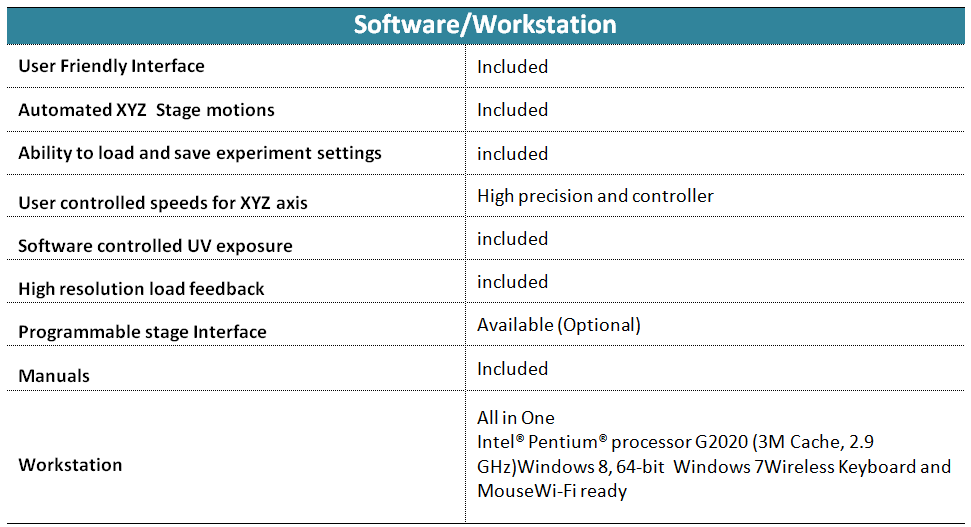
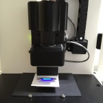
COSMOS nanoFAB is designed with a very thoughtful approach to performance, cost, and versatility. Its modular design concept allows use of the common mechanical/electrical components across different techniques resulting in ease of use and lower cost. Additionally, the modular and flexible concept allows use of future modules under development, further improving the capability and ROI. The equipment consists of a solid foundation and very accurate XYZ stages are equipped with stepper motors coupled with encoders for fine control. It comes ready with a very sensitive load cell that allows for detecting contact with the sample and controlled application of load in relevant techniques.
While the instrument is fully capable of being a research tool for rapid prototyping or experimental validation of new research, in the world of education, COSMOS nanoFAB will enforce teaching and application of concepts in surface chemistry, material science, industrial applications, electronic components, semiconductors devices, bio immobilization, and bio-sensing applications.
Module 1
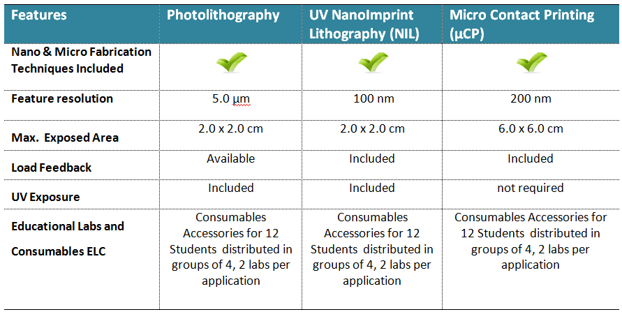
- Photolithography: Through a series of experiments, students learn the concepts and critical parameters of Photolithography: current foundation of the semiconductor industry.
- Micro-Contact Printing (µCP): Researchers could use to make prototype samples or Educators can get class acquainted with one of the oldest and lab friendly technique to pattern nano& micro scale features of organic, inorganic and bio materials.
-
Photo NanoImprint Lithography (UV-NIL): A great technique for researchers to pattern and fabricate at the nano scale, thus opening new possibilities for their existing research. On the education front, students can experience and practice NanoImprint Lithography, considered by industry experts as the most promising technique that will meet the future demands of the semiconductor industry.


